Any printed circuit board you produce should be your pride and joy. You have spent hours pulling it together and you need to know that it is going to work properly before you put it into production. Here are some of the best ways you can test your PCB design to make sure it functions as flawlessly as you intend it to.
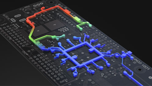
Test for PDN Issues
Power Delivery Network issues will cause you an entire host of problems and so you need to ensure that it is functioning correctly before you start your tests. One of the easiest ways to do this is by using the PDNA 2.0 Datasheet. This will analyse your entire design in the design stage itself so you can pre-emptively guard against PDN issues.
Reports from such datasheets can also help you cut costs in other ways. You will get to skip several rounds of troubleshooting and the project can move forward in a much timelier manner. With the capability to record your design at every stage of the process, you will not just be improving this particular PCB design but all of your future ones too.
Check the Simple Things
Sometimes it is little things that can cause your PCB to fail. Go through each layer of the design and check for shorts; disturbances caused by two or more overlapping traces. It is such a basic thing but it can prevent you from having a functioning circuit board.
Another thing you can do is check that the nets are connected correctly. Make sure that they are correctly attached between components so that everything will function correctly when you have built the full circuit board.
Little tests will check that your circuit board is functioning as it should do. They may seem unneeded but it can sometimes be the easiest things that we forget. A glaring mistake might be immediately obvious but only a well-trained eye will notice a small one.
Monitor the Failures
If your PCB fails during the testing phase, it can be for a variety of factors. Make sure that you are monitoring each and every test to make sure you know exactly when and where the PCB failed. If you do so, you will be able to diagnose the issue a lot more easily and you will be able to rectify it easier. This will also save you time and money in the future as your PCB won’t have to go through multiple testing rounds.
PCBs can be tricky to master and even those who have been making them for years can encounter problems. Lay down a routine for both design and testing and you will pick up issues when they occur much faster than you otherwise would. Be knowing where to look for design issues, you will be able to pre-emptively guess where the flaws are likely to be. This will make you a better PCB designer and a better electrical engineer overall.